![]() CPU emulation, particularly of older processors, is an interesting topic.
CPU emulation, particularly of older processors, is an interesting topic.
While emulation source code for various CPU cores is easily available, I wanted to better understand how to interface the emulated CPU with my host machine. Therefore I decided to write a simple example of a host system for an emulated MOS Technology 6502 microprocessor.
The goal would be to have the emulated 6502 write “Hello, world” to the console of my linux desktop machine.
Why a 6502?
I had a Commodore 64 when I was younger so was always particularly interested in the CPU of that machine, which was a MOS Technology 6510. The 6510 is a derivative of the 6502. It has an 8-bit general-purpose I/O port which the 6502 does not have, but the instruction set remains the same.
The emulated system
The emulated system is quite simple. It has some RAM and a character output device. The 6502 itself has a 16-bit address bus and 8-bit data bus, with the bus lines numbered from A0 to A15, and D0 to D7, respectively.
One way the physical version of this system could be wired is as follows: Imagine each device has an active-low ENABLE pin. In other words, when the ENABLE pin is connected to ground, the corresponding device is activated. Address line A15 is then connected to the ENABLE pin of each device. However — and this is crucial — the signal on A15 travels through an inverter before it reaches the ENABLE pin of the Output device. This is shown in the diagram below.
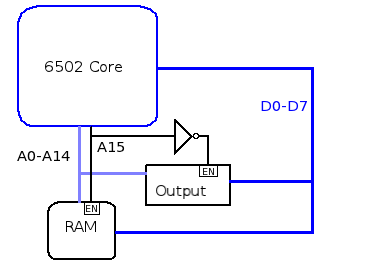
This means that all addresses in the range 0x0000 to 0x7FFF will result in the RAM being enabled (since A15 is low for all those addresses in that range) and the Output Device being disabled, and all addresses in the range 0x8000 to 0xFFFF will mean the RAM is disabled, and the Output Device is enabled (since A15 is high, but subsequently inverted before it reaches the Output Device, for all addresses in that range). This is what is meant by the statement “The Output Device is located in the 0x8000 to 0xFFFF memory space” and is known as Memory-mapped IO.
Accessing the RAM and Output Device
So now we know what addresses to read to, and write from, to access one or other of the devices. But what does each device “see” when its ENABLE pin goes low? That depends on how many of the other address lines (A0 to A14 inclusive) are connected between the 6502 address bus and the device. Imagine the Output Device has a 2-bit address bus and an 8-bit data bus. This means 4 distinct locations can referenced within the device. The technical documentation of this (imaginary) device would probably refer to these locations as Registers, numbered 0 to 3.
Let’s assume that the two address lines of the Output device are connected to A0 and A1 of the 6502 address bus. If the 6502 generates address 0x8003 on the address bus, and generates 0x65 on the data bus, the value 0x65 will be written to the register 3 of the Output device. But the same access will also take place even if the address 0x8018 appears on the bus! This is because the Output device is still enabled (because A15 is high) and A0 and A1 are high. Since the Output device is only connected to A0, A1, and A15, all other address lines are ignored. This is known as address-aliasing.
Of course, this design is very wasteful of address-space. Half of the 6502 address space is dedicated to an Output device with only 4 registers, and the CPU can only access 32KB of RAM.
Emulating the system in software
To emulate the system above, the host system software simply examines the address being generated by the 6502 CPU emulator. The software calls different functions depending on the value of the address and whether the CPU is doing a read or write. If the 6502 is performing a read, the called function will return a value to the 6502 CPU emulator; if it is performing a write the called function will take the value as one of the call parameters. In the physical system these values would actually travel over the data bus.
CPU Emulator source code
To emulate the 6502 CPU I downloaded and built Marat Fayzullin’s Marat Fayzullin‘s 6502 Portable Emulation Package. The code is an emulation of the 6502 instruction set, which processes a stream of 6502 opcodes. These opcodes set the state of the 6502 registers and status variables, just like the real processor. It can also read and write to any location in the 6502 address space. But, of course, all of this performed in software, not in silicon. Well, of course, it’s all eventually performed in silicon, but that’s where the philosophy comes in!
To interface with the 6502 emulator I had to implement a read function, and a write function. These functions are called by the 6502 emulator when the 6502 generates a read or write cycle, respectively. It is in these functions that the memory mapping is enforced.
/* Implement the system memory map for writes. */

void Wr6502(register word Addr, register byte Value)

{

/* Is A15 high? */

if ((Addr & A15_MASK) == A15_MASK) {

write_tty((char) Value);

} else {

/ * Set the location in memory. */

ram[Addr] = Value;

}

}
Creating the RAM
Adding some RAM to the system is easy — it’s simply an array of bytes, sized to the amount of memory the system has.
#define TOP_OF_RAM 0x7FFF

unsigned char ram[TOP_OF_RAM + 1];
How the Output Device works
The emulation of the Output device is trivial.
#include

void write_tty(unsigned char value)

{

printf("%c", value);

fflush(stdout);

return;

}
The hosts system code calls this function whenever the 6502 writes a byte to the first “register” of the device, located at 0x8000 in the memory space.
Hello, world!
That’s it for this post. A future post will show the 6502 assembly code that writes to the Output Device.
The Code
You can find the code on github.